MRAM Magnetic Immunity – an Empirical Study
December 2020
Introduction
MRAM technology has emerged as the top memory contender to replace embedded NOR Flash as it runs out of steam beyond 28/22nm technologies. It has been shown to be capable of higher performance and endurance metrics than embedded Flash, and it has within the last few years seen significant progress on reliability. Several companies are now offering embedded MRAM (eMRAM) IP able to withstand solder reflow and reach automotive grade retention. eMRAM is now widely seen as ready for production and the first products are starting to emerge on the market.
The main threat for the wide adoption of MRAM memories continues to be their lack of immunity to magnetic fields. The magnetic immunity (MI) level of the MRAM memory is set by the coercivity field, which is the field needed to switch a cell to the opposite state and thereby corrupt the memory content. MRAM MI level has seen significant research and improvement over the years and new data is continuously published showing improved immunity level from various MRAM vendors.
This data, however, is rarely compared to the actual magnetic field exposure scenarios which will occur in consumer applications. This can leave the SOC developers uncertain, whether the selected memory is going to be reliable over the product lifetime in their use-cases. Articles may reference some of the international standards for magnetic exposure levels of electric circuits, but, as will be shown, these standard levels are significantly below the real exposure levels which may occur.
This study will show the current state of magnetic immunity reported by the most prominent players developing eMRAM. Focus of this review is on Spin Transfer Torque MRAM (STT-MRAM) which is currently the most mature technology targeted to take over for embedded Flash. Then two specific exposure scenarios will be evaluated with respect to magnetic field strength applied to internal components, and the results will be compared to the reported MI levels from suppliers. Finally, the study will discuss future improvement paths as well as highlight some of the additional considerations memory integrators need to be aware of in their discussions with memory vendors.
The study focuses on magnetic immunity of STT-MRAM integrated in a smartphone application as NOR Flash replacement, but the results and use-cases are relevant for many different applications. Throughout the study the magnetic field strength and immunity levels will be given in Oersted (1 Oe =79,77 A/m) and a target bit error rate (BER) of 1 ppm is used throughout, unless otherwise noted.
Embedded MRAM Magnetic Immunity Overview
As with any memory module, the native performance and reliability is dictated by the bitcell. This central point in the MRAM memory is the magnetic tunnel junction (MTJ), which for almost all STT-MRAM modules are implemented in the backend process as a vertically stacked perpendicular MTJ (pMTJ). MRAM modules can be targeted at different applications, such as Flash or SRAM replacement, depending on the design choices made for the MTJ. This choice dictates read/write performance as well as reliability aspects for the memory. Several articles referenced in this study highlight the impact of the MTJ process stack as well as the balance of memory logic states on the achievable MI level.
The MI level of eMRAM memory has several external dependencies outside the direct field strength. Articles show a strong dependence of MI to temperature, field angle and exposure time. The state of the memory also plays a role in determining how susceptible it is to magnetic fields.
Table I below shows a collection of MI levels captured from scientific articles and datasheets from the last few years. Comparing the data directly is difficult, as different assumptions and metrics are used by the authors. In addition, some articles are missing key information, which has meant that certain assumptions are needed to create a table like the one below.
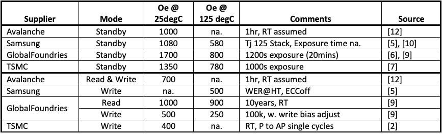
Table I: Reported MRAM MI levels @ 1ppm BER for Standby & Active modes vs. Temperature
Although all numbers have been derived for 1ppm BER level and roughly the same temperature, it is very difficult to compare the above numbers or to quantify what level is sufficient. When looking at the active MI levels even more discrepancies exists as measurement conditions and operation sequences start to play a role. The table also serves to illustrate how important it is to understand the conditions and assumptions which produced the results. Since each of these vendors are developing their own proprietary MTJ stack, often with help from technology partners, the trend curves wrt. e.g. exposure time and temperature may also differ between offerings.
Recently TSMC and GlobalFoundries have published a more complete set of standby MI levels vs. exposure time and temperature, and provided their own extrapolation to 10-year exposure levels. This can allow for some comparison. Below these levels are plotted again adjusted to 1ppm BER level.
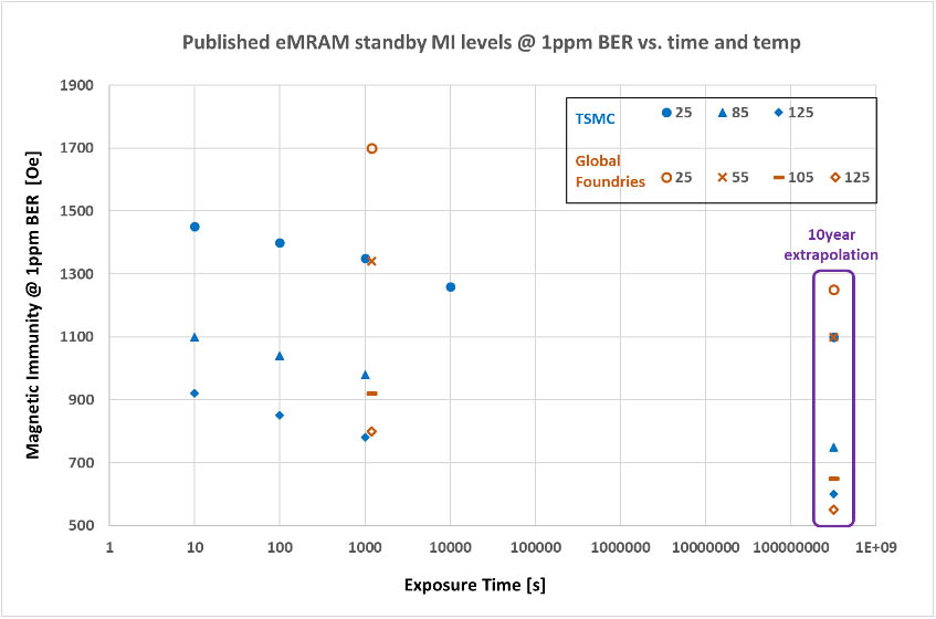
Figure 1: MRAM MI levels from GlobalFoundries and TSMC with 10-year extrapolation [7], [9]
Both foundries provide a solution which is able to tolerate > 1000 Oe at 25degC for 10-year exposure, while keeping the BER at a manageable 1ppm. However, for a smartphone application where the average internal temperature is likely above 55 degC, the MI levels may drop below 1000 Oe.
These results are also reflected in the Magnetic Immunity Guideline published by GlobalFoundries, which does a good job summarizing their technology capability in terms that are common in NVM reliability considerations. In this 2020 IRPS article GlobalFoundries, and their MRAM development partner Everspin, provide one of the most complete and competitive MI level overviews [9]. This table, repeated below as Table II, can be used as a benchmark towards other eMRAM suppliers, who should be encouraged to post similar performance statistics, a topic discussed later in this study.
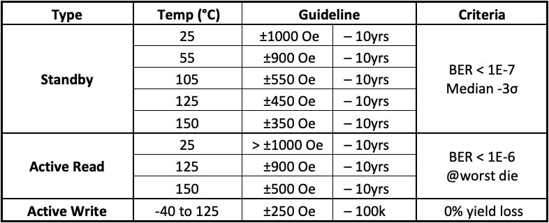
Table II: Magnetic Immunity Guidelines from GlobalFoundries eMRAM offering [9]
Note that the active mode immunity levels in this table assume active bias adjustments in read and write mode to compensate for temperature and/or magnetic field levels, which may result in a performance or cost penalty for the memory block.
In this chapter the most recent MI levels have been reported for eMRAM modules targeting eFlash replacement. Most suppliers of eMRAM modules are now capable of providing eMRAM offerings with more than 1000 Oe MI at RT in standby. However, there are subtle differences in the overall performance of the offerings, which makes it difficult to compare offerings wrt. exact MI level achieved.
It should be noted that this study summarizes results from suppliers reporting some of their best achievements so far. Most of the eMRAM offerings reported are able to withstand solder reflow and have >10 years retention @200degC. As mentioned, there are other MRAM offerings with a different tradeoff wrt. long term reliability and operation performance, which will also be discussed at the end of this study. These memories may have lower MI levels compared to what is presented here.
The following chapter will zoom in on two real life scenarios, which should be considered for most SOC developers prior to integrating MRAM memory.
Worst Case Magnetic Field Exposure Scenarios
The main purpose of this study is to couple the MI levels of eMRAM modules available today to the worst case magnetic exposure scenarios that can occur in real life.
Some of the published MRAM articles show compliance with international standards wrt. magnetic exposure for electronic circuits. Shown below are two standards referenced by MRAM suppliers in their material, along with the MI compliance level in Oe.
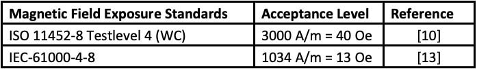
Table III: Standards for magnetic exposure of electrical components
However, based on this analysis, these standards accept significantly lower magnetic field exposure than what can be expected from real scenarios. Hence the ability for the MRAM to comply with these standards adds little to no value for SOC developers, and all MRAM suppliers referenced here have shown to easily meet these restrictions in both standby and active mode.
As a more relevant alternative, we will here consider two other scenarios as worst-case scenarios, assuming a smartphone application:
- DC field exposure from rare-earth magnets
- AC field exposure from wireless charging pads
These two scenarios will show how close the magnetic field exposure is to the reported MI levels.
DC Field Exposure from Rare Earth Magnets
Exposure from powerful rare-earth magnets are often published as malicious attack scenarios in articles [1], [11]. However, in widely available smartphone holders there is a normal use-case, which puts smartphone components in close proximity to rare earth magnets for long periods of time. These holders work by placing a thin metal disc on the phone or case, which provides the magnetic attraction needed to hold the phone in place. The metal discs may provide some shielding and limited mechanical spacing to the magnets; however, memory circuits in the phone can also be located outside the area of these discs.
Below is a small selection from Amazon of such holders, all using various amounts of Neodymium magnets and all available at around $10-20.
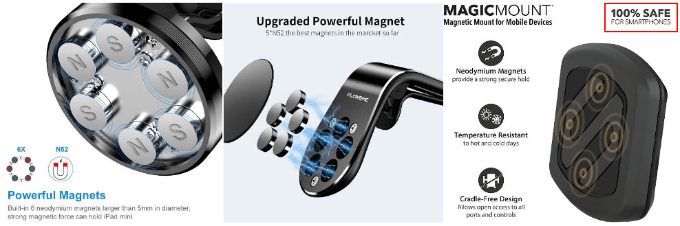
Figure 2: Selection of phone holders using strong Neodymium magnets
Note that some manufactures claim that they are safe for smartphones, as shown in red above.
N52 Neodymium magnets are considered the most powerful magnets available. Depending on dimensions the surface magnetic field of these magnets may reach over 5000 Oe at the surface. When used in e.g. a car, the phone and its components can be placed in such a holder for several hours per day. If used as stands in homes, the components may be exposed to these fields for days or weeks. The exposure in this scenario can therefore be significant.
As an example, we used the published data from one of the Neodymium manufacturers [18] to gauge the strength of such magnets. Two magnets with a surface field strength of 5000 Oe (N52 5mm x 2.5mm) and 3500 Oe (N48 5mm x 1.5mm) were checked for various distances applicable to components in a smartphone sitting in such a holder.
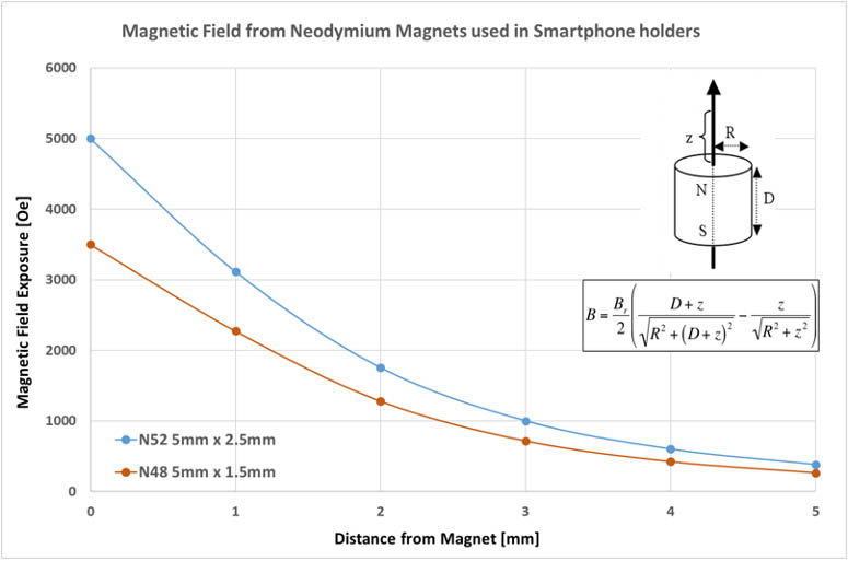
Figure 3: Neodymium magnetic field vs. distance to components - Formula from [18]
Although the magnetic field quickly deteriorates, components within 2-3 mm of the magnet surface are still experiencing field strength of 1000-2000 Oe. This is above what the MRAM technology is capable of handling today in standby mode at high temperature, and also exceeds the capability for almost all suppliers in active mode. Additionally, some safety margin will need to be applied to account for directional differences, which will be discussed in a later section.
As mentioned, most MRAM suppliers consider this a malicious attack to the memory rather than a valid and normal use-case. Since there are no good technical solutions to prevent memory corruption in this extreme case, considering it an extreme event allows for suppliers to limit exposure time or conditions in their research. This is however a valid use-case, which is widely used for long periods of time and is broadly promoted as safe for smartphones and electronic components. At the end of the study, we will discuss some potential paths for mitigating this effect as well as some additional topics to consider when integrating MRAM.
Next, we will consider AC magnetic fields generated from another common smartphone use case.
AC Field Exposure from Wireless Charging Pads
Wireless charging has become increasingly popular for almost all electronic devices. This simplifies the charging process for the user and allows the manufacturers to completely enclose their device for better protection against the environment. Wireless chargers are becoming more powerful to a point where they could threaten MRAM data integrity when charging certain electronic devices.
Similar to the phone holders described above, wireless charges are widely described as being safe for smartphones. The number of articles claiming that wireless charging is safe for smartphones complicates the communication to the user, should this no longer be the case with MRAM onboard.
Quantifying the magnetic field exposure from wireless chargers is not a trivial task as manufacturers do not publish field strength data from their individual products. However, the Federal Communications Commission (FCC) specifies a maximum human exposure to magnetic fields generated by devices according to the Maximum Permissible Exposure (MPE) levels set in FCC CFR 47 sec. 1.1310 [14]. The FCC also provides a product test guideline against this requirement, which is described in the FCC KDB 680106 [15]. For wireless chargers to be compliant, this guideline specifies a maximum exposure measured 15cm sideways or 20cm above the source of 50% of the maximum MPE level for the relevant frequency range. As wireless chargers operate typically between 100 and 200kHz the MPE level is set at 1.63 A/m according to the guide, meaning the FCC compliance level is 0.815A/m. This level appears very low, and in fact much lower than the above referenced component standards, but due to the measurement distance the exhibited magnetic field strength at the charging pad level, may be close to the MI levels of some MRAM modules.
On the FCC website the detailed measurement reports and achieved results wrt. magnetic field exposure are available for a range of wireless charger approved for the US market. As the magnetic field decreases quadratically with distance, this data can provide a rough estimate of the magnetic field exposure applied to mobile phone components placed directly on a wireless charger. This can provide a guideline as to how concerning the wireless charging scenario is for eMRAM memories.
Consider as an example an embedded MRAM located in a chip inside a smartphone placed on a wireless charger. Below are shown the measurement setup for a Belkin 15W QI wireless charger pad and the test setup used.
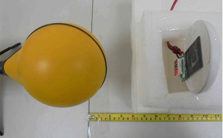
Figure 4: FCC test setup to measure magnetic field exposure from wireless chargers [16]
This test setup uses a mechanical load, which limits the amount of shielding caused by an actual smartphone, and is therefore more realistic for this scenario. The measurement has been conducted with and without a 3mm gap between the load and the source to create the worst-case load on the charger, this has however only minor impact on the exposure. The highest measured magnetic field from the wireless charger at a distance of 20cm was 0.4168 A/m (w. 3mm gap) and 0.4032 A/m (without gap) [16].
Using this measured data and the quadratic attenuation of magnetic fields with distance we can calculate the magnetic field exposure just mm from the wireless charging pad coil. Below are plotted the exposure levels (converted to Oersted) for the mentioned Belkin 15W wireless charger, a less powerful Belkin 5W wireless charger [17], as well as the FCC compliance limit of 50% of MPE.
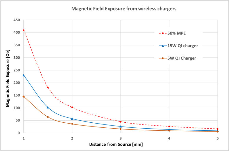
Figure 5: Estimated magnetic field exposure from wireless chargers & FCC compliance limit
The smartphone components are estimated to be 2mm from the field source, given that both smartphone and wireless chargers are enclosed in material and the wireless antenna of the smartphone is typically located as close to the case as possible. For this worst-case consideration, we will not consider additional attenuation from charger or smartphone materials, outside the pure spacing.
With a component distance of 2mm from the source, the concerns wrt. magnetic immunity are roughly 20x less than was the case with a static magnetic field from Neodymium magnets. Even for a charger performing at the FCC compliance level, the components are only subject to roughly 100 Oe field strength at this distance. Comparing to the reported MI levels for eMRAM offerings presented here, they all should be able to work in such a field in standby and active mode, and even at elevated temperature which are common during wireless charging.
Finally, it should be mentioned that the worst case exposure level is more than double the ISO Automotive guideline for component exposure and 8x the IEC guideline for consumer electronics. As mentioned, compliance to these standards bring little insurance that the memory will function reliably in everyday use-cases.
Technology Improvements, Magnetic Shielding and Other Topics
In this section some additional topics and findings will be reported, which emerged during the research for the study. This can give a hint as to future development for MRAM improvement or to topics which needs to be considered when selecting and integrating MRAM in products.
Technology Improvements on the Horizon
The MI level of MRAM is still being researched and improvements are expected, as the MTJ design is improved and the memory technology matures even further. There are articles showing better immunity can be achieved, if e.g. manufacturing can improve the balance of energy barrier (Eb) between the two states in the MTJ [9]. This however often comes with a tradeoff on performance and/or write power.
The MRAM offerings considered here are aimed at Flash replacement, as mentioned, with most of them able to sustain data integrity during solder reflow and reach automotive level retention requirements. Different MRAM types and offerings are available as e.g. persistent memory or SRAM replacement, which sacrifices some reliability metrics for higher performance. As an example, Everspin specifies a minimum MI level of 25 Oe for some of their products [13], which would likely not be able to sustain data, if placed closer than 3mm on a powerful wireless charger.
Finally, there has been ongoing research in active handling of external magnetic fields. Articles have been published, which suggests using a MTJ with lower coercivity field as a sensor along with the regular MTJ bitcells to sense an approaching magnetic field [11]. This would allow the memory to switch to a safe mode, either by canceling ongoing operations and putting the memory in standby, or by increasing bit error detection and correction through ECC. These do however require the memory to be powered and operational to take effect, which is why lower MI levels may be acceptable in active mode vs. standby for some applications.
Overall, the result of these next technical improvements is still to materialize. However as long as the industry remains skeptical of MRAM, which is hindering the widespread adoption and integration into new products, MRAM suppliers will need to continue seeking improvements to their offerings.
Magnetic Shielding
In further efforts to improve MRAM MI level, several companies are researching magnetic shielding as part of the packaging, and e.g. Everspin includes magnetic shield in the packaging of all their discrete MRAM products today [13]. Effective shielding does however increase cost and complexity of packaging. In addition, there may be product restrictions on e.g. the board build height, that would be unable to comply with an additional shield thickness even at a fraction of a mm. It is therefore important to prove that the additional complexity and cost of a shield provides value for the user.
Magnetic shielding is seen as one of the only effective ways to reduce the impact from an external magnetic field. A BER reduction of 106 has been reported for very strong external fields applied directly at the package [7], however specific data on conditions for this result are limited and the shield in this case is only protecting the top of the die.
Most of the reported articles deal with a magnetic field applied 90deg to the die, however data is presented which suggests that BER levels of STT-MRAM increase by more than 50x, when fields are applied at 45deg angle vs. 90deg [5]. Judging by the slope of BER vs. magnetic field curves this added effect from the angle roughly corresponds to a reduction in MI level of 150 – 200 Oe, provided the field is applied at the same distance. Therefore, additional margin should be considered and applied when evaluating MI levels from MRAM modules measured at 90deg. Solutions for effective shielding surrounding the die are also reported [3]. These also show good improvement, but significantly complicates die packaging and connections.
For very strong fields shielding may only provide limited protection. There is evidence showing that the efficiency of the shield drops, when the field strength approaches the MI levels mentioned here. This means that the shield no longer provides additional protection as shield thickness is increased, in this case saturating at 65% efficiency for an 800 Oe field regardless of thickness [4]. Clearly shielding of MRAM memories, be it in die, package or application still needs significant research.
Overall shielding of external magnetic field is possible and can provide some protection, provided your application will allow for it and there is a good understanding of the fields and scenarios your product will be subjected to. It does however add significant cost and complexity, and there is today no one-size-fixes-all solution available for shielding embedded MRAM.
To justify adding a magnetic shield to the application, customers will need to determine the gained improvement empirically depending on their application use-case and packaging choices.
Acceptable BER vs. Module Failure Rate
The BER level is closely linked to the MI level of the memory, and in this study a 1ppm level has been used throughout as a guideline for comparison. The right BER level to use depends on the application quality level targets, amount of ECC available for correction, and module size. In the reported articles there is a very steep relationship between BER and resulting MRAM MI levels, such that a small change in field strength results in significant change in BER.
This means that increasing BER target from e.g. 1ppm to 0.1ppm only marginally increases the MI level. On the other hand, a small increase in field strength from e.g. angle or field fluctuations may result in a large increase in BER level and resulting in significant module failure rate.
Given a certain BER for the failure mode, the module failure rate depends on the configuration and ECC level to correct for that failure. For a 16Mbit MRAM module with 128bit word and a standard 2bit ECC scheme available for correction, a 1ppm BER level results in less than 0.1ppm module failure rate. However, at 10ppm BER the module failure rate increases by 3 orders of magnitude. This is illustrated on the curve in Figure 6 below, which assumes random distribution of bit failures.
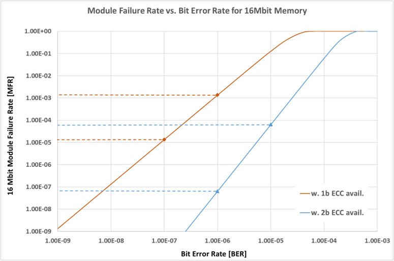
Figure 6: Module Error rate vs. BER for different ECC levels
The full ECC may not be available to correct bits affected by this failure mode. As MRAM has a stochastic write probability, as well as other long term reliability effects, part of the ECC algorithm may already be used to compensate for these other effects. Figure 6 above also shows the impact should only 1 bit be available for ECC correction. Even with a BER of 0.1ppm, the resulting module failure rate is over 2 orders of magnitude higher vs. a 1ppm BER with the full 2bit ECC. The overall ECC budget, i.e. assumptions on the required ECC width wrt. production yield, lifetime usage and expected reliability level, should be discussed with your memory supplier.
For SOC developers to fully gauge the module failure rate implications, the provided BER level needs to be the natural bit error rate without prior ECC correction. This is assumed in this study but is not stated specifically for all data presented here. SOC developers also need to check with suppliers what ECC usage is assumed in the other provided memory reliability data, as this can have a direct impact to their product lifetime reliability if not matched in the application.
Other Considerations to Improve Wide Adoption
As MRAM technology has become more mature and reliability has started to match or even exceed Flash in many areas, the MI levels of a given MRAM offering is perhaps the only real concern left for customers – and with good reason. This study shows that even the best offerings are not able to sustain operation reliably in worst case scenarios. MRAM suppliers may argue that certain use-cases are not permitted in strong magnetic fields, but limiting the user in this way is likely not feasible for SOC developers.
To gain wide adoption MRAM suppliers need to address this topic in a more structured way. The immunity guideline given in Table II is a good starting point. This provides a clear specification, which can be used directly by customers to evaluate their risk against the worst-case use. Although the actual numbers are lower than what is needed for todays applications, the table clearly summarizes the lifetime performance over temperature for the different modes at specific BER levels.
Unfortunately, the data in the table is not available from most of the MRAM suppliers, but it could be a standard requirement for MRAM datasheets. Developers should be encouraged to engage with their MRAM supplier to collect this data for their offering wrt. standby, but especially wrt. active operation. This data should be evaluated while keeping topics like application temperature, exposure over lifetime, additional margin for field fluctuations and specific application use-cases or constraints in consideration. Ideally MI would become a standard MRAM reliability metric governed by reliability standards similar to other well-known NVM reliability metrics.
Conclusion
The study presents an overview of best-in-class MRAM offerings targeting embedded Flash replacement at the time of writing. Most offerings are able to reach standby MI levels of 1k Oe over extended time, however the MI level of active operation is much lower especially for write operation, reaching levels of 250-500 Oe across temperature.
Two critical use-case scenarios for embedded MRAM integrated in a smartphone application have been considered. The most significant threat is from exposure to Neodymium magnets, which can cause magnetic fields above the reported MRAM MI levels. The presented use-case is widely available, low-cost and used for extensive periods of time. This should be considered a real threat to normal MRAM use, and, unless the scenario can be completely avoided, solutions should be implemented to cope with this effect.
Active fields from wireless chargers are unlikely to have an impact on the MRAM offerings presented here. However, this threat should still be considered in applications using MRAM with a different reliability tradeoff, which may be susceptible to fields below 100 Oe. These use-cases exceed the standard requirements for electronic components both in consumer and automotive environments.
Overall adoption of MRAM memories continues to be limited by the MI performance of the technology, and with good reason. Judging by the data presented, the native performance of the memories is still not able to guarantee reliable performance in these common use-cases, and there is no simple solution to mitigate the threat from such external fields. Some applications may try to restrict use-cases or control the environment to allow for MRAM memories to perform, while others may need to implement costly shielding or complex active measures.
As highlighted, there are a lot of considerations to take into account when using MRAM memories, and a close technical relationship with the MRAM suppliers is needed for products to become successful. Should you need expert assistance for your development in this complex field, MemXcell can help you and your team evaluate the tradeoffs and find the right solutions. We can also interact directly with the MRAM suppliers on your behalf to make sure the memory performance and reliability match your requirements and support your application.
In order for MRAM to become a successful replacement for Flash and the industry to fully emerge in wide-spread use of MRAM, the technology needs to improve MI level by roughly 2-4x without sacrificing performance. The target MI levels should be roughly 2k Oe for standby (10yr) and at least 1k Oe for active mode (100k – 1M write cycles) with a BER level below 1ppm (ECCoff). These target requirements are listed in Table IV below.
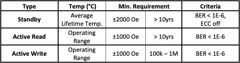
Table IV: Target MRAM magnetic immunity levels
These targets will still not permit MRAM modules to fully withstand deliberate magnetic attacks or tampering, as magnets, fields and distances in this case always can be chosen to generate significant data corruption. The application must be able to detect and actively deal with such effects.
While we wait for this level of improvement, MRAM suppliers should be encouraged to report MI levels in a uniform or standardized way in their documentation, as well as develop standard reliability flows for quantifying MI levels to their customers. This will allow the SOC developers to properly gauge product reliability and risk, and develop solutions specific to their offerings. As there are no good alternative solutions for embedded memory in advanced nodes, the incentive to create solid and standardized data to mitigate this risk should continue to grow.
About MemXcell
MemXcell provides expert consulting to system-on-chip (SoC) development teams who are integrating embedded non-volatile memory (eNVM) IP into their products.
Our expertise spans all NVM technologies, from charge-based flash and MTP/OTP to emerging memories like RRAM and MRAM. We have extensive experience in mobile, IOT, security, and automotive applications.
MemXcell offers highly skilled assistance through all phases of product development, helping you to beat your competitors in the marketplace.
Contact us if you have questions about this study, use of MRAM and MRAM technology in general, or to hear more about our services. You can also read more on the memxcell.com website, or follow us on LinkedIn for new updates and articles.
Disclaimer
This study and the data here-in are provided free of charge as is. Readers are encouraged to procure and read referenced articles and material for more detailed information.
MemXcell is not responsible for correctness of data from referenced articles or conclusions made based on this study. MemXcell is not paid or affiliated with any of the MRAM or product suppliers referenced in this study at the time of writing.
References
[1] A. Holst et. al., “Investigation of magnetic field attacks on commercial Magneto-Resistive Random Access Memory”, 2017 18th International Symposium on Quality Electronic Design (ISQED)
[2] C. Wang et. al., ”Impact of external magnetic field on embedded perpendicular STT-MRAM technology qualified for solder reflow”, 2017 IEEE International Electron Devices Meeting (IEDM)
[3] B. Bhushan et. al., ”Enhancing Magnetic Immunity of STT-MRAM with Magnetic Shielding”, 2018 IEEE International Memory Workshop (IMW)
[4] K. Lee, et. al., “22-nm FD-SOI Embedded MRAM with Full Solder Reflow Compatibility and Enhanced Magnetic Immunity”, IEEE Symposium on VLSI Technology (2018).
[5] Y. Ji et. al., ”Reliability of 8Mbit Embedded-STT-MRAM in 28nm FDSOI Technology”, 2019 IEEE International Reliability Physics Symposium (IRPS)
[6] V. B. Naik et. al., ”Manufacturable 22nm FD-SOI Embedded MRAM Technology for Industrial-grade MCU and IOT Applications”, 2019 IEEE International Electron Devices Meeting (IEDM)
[7] W. J. Gallagher et. al., ”22nm STT-MRAM for Reflow and Automotive Uses with High Yield, Reliability, and Magnetic Immunity and with Performance and Shielding Options”, 2019 IEEE International Electron Devices Meeting (IEDM)
[8] Y. Chih et. al., ”A 22nm 32Mb Embedded STT-MRAM with 10ns Read Speed, 1M Cycle Write Endurance, 10 Years Retention at 15degC and High Immunity to Magnetic Field Interference”, 2020 IEEE International Solid- State Circuits Conference - (ISSCC)
[9] T. Y. Lee et. al., ”Magnetic Immunity Guideline for Embedded MRAM Reliability to Realize Mass Production”, 2020 IEEE International Reliability Physics Symposium (IRPS)
[10] Y. Ji et. al., ”Reliability of Industrial grade Embedded-STT-MRAM”, 2020 IEEE International Reliability Physics Symposium (IRPS)
[11] J. Jang et. al., ”Self-correcting STTRAM under magnetic field attacks”, 2015 52nd ACM/EDAC/IEEE Design Automation Conference (DAC)
[12] Avalanche Technology AN000002 ”Endurance, Data Retention and Field Immunity of STT-MRAM” rev. B.
[13] Everspin Technologies EST02880 ”Magnetic Immunity for Everspin MRAM” Dated 073115
[14] FCC CFR 47 part 1 1.1310 “Radiofrequency radiation exposure Limits” v. 10-1-10
[15] FCC KDB 680106 “RF Exposure considerations for Low Power Consumer Wireless Power Transfer applications” v. 03 April 9, 2018
[16] FCC RF Exposure Test Report No. SA2002004D01 March 2020 – Belkin 15W QI Wireless charger
[17] FCC RF Exposure Test Report No. SA180709D11 July 2018 – Belkin 5W Wireless charger
[18] Information and spreadsheet from https://www.supermagnete.de/eng/faq